MEASUREMENT METHODS
Hardness and elastic modulus measurements by instrumented nanoindentati on (ISO 14577-1:2015)
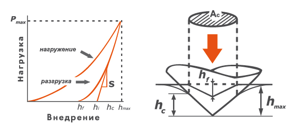
The method of dynamic nanoindentation has been implemented in “NanoScan”devices. The algoritm is based on measuring and analysis of indentation loaddisplacement data. This technique underlies the international standard of harness testing ISO 14577. The typical expiremental curve of load (P) versus depth (h) is shown on Fig. 2. It contains loading and unloading parts of the curve.
In this method hardness of a sample is defined as the maximal indentation load Pmax devided by the project contact area Ac.
Reduced elastic modulus value is inversely . Constant β depends on indenter geometry. Contact stiffness S is determined by the angle of slope of the tangent to the unloading curve in the point Pmax .
Contact area at maximal load Ac is
determined by indenter geometry and contact depth hc and it is described by the tip geometry function Ac=f (hc).
General view of the loading curve and contact diagram with designations of values used in the method for calculating the modulus of elasticity and hardness.


Hardness measurement by sclerometry (scratch application and analysis)
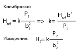
Scratch hardness testing in the “NanoScan” devices consists in producing scratches on the sample surface with a subsequent imaging of the resulting scratch traces. Obtained scratches can be scanned after with using AFM/SPM mode. Before measurements, the indenter shape is calibrated on a reference sample using the series of scratches at several defined loads. The material hardness value is calculated in comparison to the reference hardness as a proportion between the loads and widths of scratches on both the tested and reference materials. Normal and lateral creep recovery of the materials are defined using a scratch diagram. The comparative tests show good correlation for this technique with other hardness measurement methods (Table 2).
Table. Comparison of hardness measurement methods

Image of residual scratch trace allows to analyze pile-ups around the image.
Scratch method takes account of the impact of the pile-ups’ dimensions
Scratch method takes account of the impact of the pile-ups’ dimensions
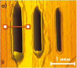
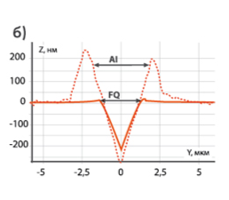
Examples of cross-sectional scratch profiles for fused quartz (solid line) and aluminum (dashed line). The arrows indicate the width of the indenter's contact area with the material during scratching.
Mechanical properties map display
Scanning NanoScan nanohardness meters allow obtaining images of three-dimensional surface topography by scanning probe microscopy. Scanning is performed in the semicontact mode by a diamond indentor fixed on a piezoceramic probe. The probe makes resonant vibrations at a frequency F ~10 kHz and with an amplitude A < 50 nm. During scanning the frequency F or the amplitude A of oscillations is kept constant.
Oscillatory mode of the probe operation allows to obtain additional information on the structure and mechanical properties of the investigated samples in addition to the relief image. In the process of scanning simultaneously with the relief height the change of the free parameter of the probe oscillations is recorded (when scanning with constant frequency F the free parameter - amplitude A, and vice versa). The obtained image is a map of visco-elastic properties distribution over the surface. This mode allows to study the structure of multiphase materials, as well as the distribution of mechanical inhomogeneities on the surface.
The map of mechanical properties distribution obtained in the process of scanning is relative and provides only qualitative information about the absolute values of mechanical parameters. Quantitative measurements of the modulus of elasticity (Young's modulus) at given points of the surface under study can be carried out by force spectroscopy.
Construction of the mechanical properties profile
Mechanical testing of micro-objects
The automation of a series of measurements along a given line or on a given area on the surface of a sample allows the NanoScan instruments to implement methods of mapping or profiling mechanical properties.
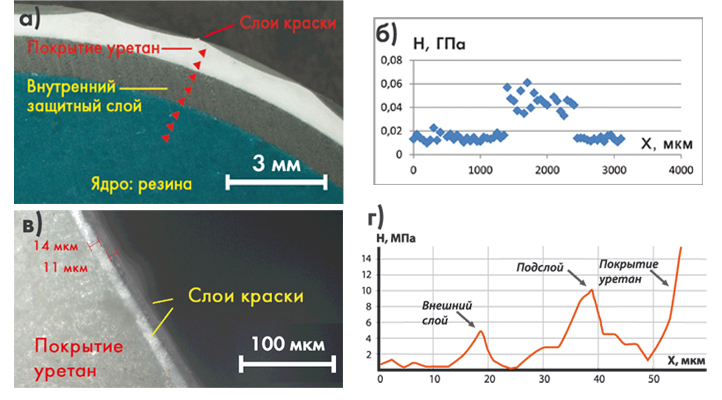
This technique is extremely important when studying objects, the structure of which is characterized by significant spatial heterogeneity of mechanical properties. An example of such an object is a golf ball, consisting of a core and several layers and coatings with thicknesses ranging from a few micrometers to a millimeter or more (a). Measurements can be taken either in air or in a liquid medium.
This technique is extremely important when studying objects, the structure of which is characterized by significant spatial heterogeneity of mechanical properties. An example of such an object is a golf ball, consisting of a core and several layers and coatings with thicknesses ranging from a few micrometers to a millimeter or more (a). Measurements can be taken either in air or in a liquid medium.
High accuracy of mutual positioning of the object and indentor, as well as the possibility to use indentors of different geometries allow testing mechanical properties of micro-sized objects in NanoScan devices. In particular, a technique has been implemented to determine the mechanical strength of polyelectrolyte microcapsules obtained using layer-by-layer adsorption (LbL) technology based on alternate adsorption of polycations and polyanions on a charged substrate.
The characteristic diameter of the objects can range from units to hundreds of micrometers. The exact geometric characteristics of the object are determined from the optical microscope image. A diamond flat die with a given working diameter is used as an indenter.
The load-displacement relation registered allows to determine the force at which the capsule fracture occurs. The force-displacement relationship determines the mechanical strength characteristic of the capsule.
A similar technique is widely used for biological objects, ink particles used in printer toners, and tests of fine abrasive material.
The NanoScan software allows to automatically measure and build images of profiles and maps of hardness and modulus of elasticity distribution in the field from a few tens of micrometers up to 100 mm with a specified step between points. Examples of measured profiles are shown in Fig. b and d, the results of measuring the properties of each layer are given in the Table:
Positioning of the object by video image (a), microphotograph of diamond indenter of "flat die" type (b), load-displacement relation registered during microcapsule compression (c)
Optical photographs of the sample and hardness profiles. Core, inner layer, urethane coating (a),(b); urethane coating and two layers of paint (c),(d).

Vickers microhardness measurement
Nanohardness tester "NanoScan-4D" and Vickers hardness meter "NanoScan-HV" allow to measure microhardness by recovered imprint in accordance with GOST 9450-76. Four-sided Vickers-type pyramid (angle between opposing faces 136°) is used as an indenter. Measurements are made on the basis of optical microphotographs. The hardness HV is calculated as the ratio of the maximum load applied to the indenter to the surface area of the recovered indentation measured from its image:
d – the average length of the diagonals of the quadrangular print, mm, P — maximum load in kilogram-force.

Examples of Vickers imprints on different materials. a - tool steel, b - bronze, c - zinc oxide ceramic
Measurement of the temperature dependence of mechanical properties
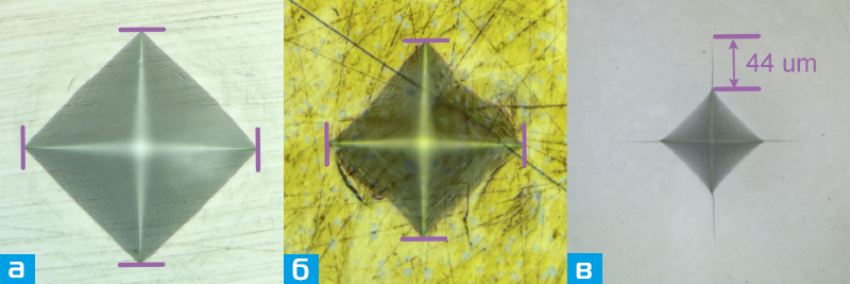
NanoScan micro-hardness testers enable the automatic dimensioning of indentations using an intelligent machine vision system. If there are cracks in the corners of the Vickers indentation, it is possible to calculate the crack resistance of the sample at the indentation point. Vickers hardness is one of the most common and longest-used hardness determination methods in the world. Its use in combination with nanohardness methods allows direct comparison and referencing of hardness values at different scales.
The sample stage with heating control is used to measure mechanical properties of materials at elevated temperature. The sample can be heated to a temperature of 400 0C and all types of mechanical tests implemented in the NanoScan-4D hardness tester can be carried out. The accuracy of maintaining the specified temperature is 0.1 0C. The tests are used to measure such material characteristics as hardness, modulus of elasticity, coefficient of elastic recovery, crack resistance, wear resistance and a number of others at a given temperature. Typical sample dimensions for temperature tests with NanoScan are 25 x 25 x 10 mm. As an example of experimental dependence of mechanical properties of the material on temperature in figure a,b graphs of dependences of hardness and elasticity modulus on temperature for polymethylmethacrylate (PMMA) when heated to 140 0C are presented.

Dependence of hardness and modulus of elasticity of PMMA on temperature (a); Load-displacement dependence at 30 0C and 100 0C obtained on PMMA sample (b).
Tomography of mechanical properties
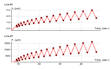
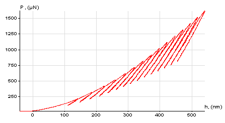
The traditional indentation method (ISO 14577) determines the mechanical properties of the material in one area at one depth. The devices of NanoScan series implement the method of multi-cycle loading with partial unloading technique, which allows to measure the mechanical properties at different depths during one indentation into the surface of the sample. In this method, the unloading is carried out to a certain fraction of the value of the maximum load, and at each subsequent cycle the loading is repeated by a larger value Fig. 1, Fig. 2.
Fig. 2 Dependence of loading force on indentation depth for multi-cycle indentation.
Fig. 1 Timing diagram of indenter plunge depth and loading force during multicyclic indentation.
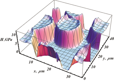
In devices of NanoScan series the method of tomogram of hardness and modulus of elasticity of the near-surface layer of the sample is implemented. The method is based on a combination of two methods: the method of multi-cycle loading and the mapping method (plotting a series of indents in a square grid), which allows obtaining the distribution of mechanical properties of the material in the volume (tomogram). A tomogram can be plotted on a sample surface up to 10 cm in size and up to 10 µm in depth. The resolution of the instrument allows to start measuring mechanical properties at depths of several tens of nanometers. Lateral resolution is determined by the size of plastic imprints remaining after loading tests and is in the order of tens of microns.
Dynamic stiffness measurement
The NanoScan-4D devices implement the method of dynamic measurement of contact stiffness. This method is based on the measurement of quadrature components of displacement when a harmonic force is applied, in addition to monotonic deepening of the probe into the sample. On the basis of obtained data the values of real and imaginary stiffness components are calculated and then E' and E'' values corresponding to in-phase and displacement component shifted by 900 are calculated on their basis. The typical operating frequency range is up to 50 Hz, but in the case of preloaded measurements it is possible to operate at frequencies up to 300 Hz.
Dynamic hardness measurement
Measured values of elastic modulus E' and loss modulus E'' for fused quartz (a), bitumen (b) .

The standard nanoindentation method implemented on the basis of ISO 14577 is based on the determination of hardness and modulus of elasticity from the slope of the unloading curve, the maximum load and the indentation depth. A number of methods now exist which combine oscillating oscillating motion with indentation penetration into the specimen, allowing for depth dependent measurement of modulus and hardness. A similar approach can be used to obtain maps of the elastic properties of the material.
The NanoScan devices employ the method of multi-cycle loading with partial unloading, which also allows to obtain hardness and modulus of elasticity depending on the depth of indentation; however, it should be noted that all these methods use information on the indenter shape, and thus are strongly affected by roughness influence on the measured result. The proposed method of dynamic hardness measurement is significantly less affected by surface roughness, but requires a priori information about the value of the modulus of elasticity, as it actually allows to measure the H/E2 value. The final dependence, which allows us to produce this value from the experimental data, is as follows:
The NanoScan devices employ the method of multi-cycle loading with partial unloading, which also allows to obtain hardness and modulus of elasticity depending on the depth of indentation; however, it should be noted that all these methods use information on the indenter shape, and thus are strongly affected by roughness influence on the measured result. The proposed method of dynamic hardness measurement is significantly less affected by surface roughness, but requires a priori information about the value of the modulus of elasticity, as it actually allows to measure the H/E2 value. The final dependence, which allows us to produce this value from the experimental data, is as follows:

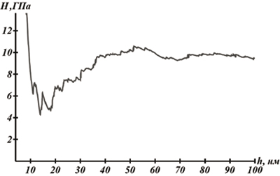
where F and Δf are the force and the shift of the resonance frequency measured during scanning, f0 and k are the resonance frequency of oscillations of the free probe and its dynamic stiffness. The last two parameters are determined in the process of calibration of each probe and are considered to be constant during further work. Using this expression, the dependence, H/E2 (and, respectively, H or E if at least one of these values is known), can be plotted as a function of depth or surface coordinates. Below are examples of hardness vs. depth measurements, for measurements on fused quartz, as well as hardness maps for fiberglass in an epoxy matrix. In both cases, the values of the modulus of elasticity were known from other sources.

The actual and imaginary parts of the complex modulus of elasticity are determined by the following relations:
where А — contact area,

— contact stiffness;
, where С — coefficient of viscous friction.


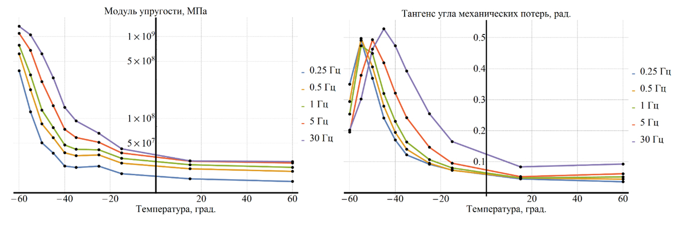
The figure shows an example of the dependence of the modulus of elasticity and the tangent of the angle of mechanical losses on temperature and frequency.
Dynamic Mechanical Analysis (DMA)
Dynamic Mechanical Analysis (DMA) is a test technique and tool used to study the dependence of mechanical and viscoelastic properties of materials on temperature, time and frequency when subjected to periodic loads. As a rule, the technique is applied to polymeric materials. In the NanoScan series, this technique is implemented using a spherical tip that is embedded into the specimen surface. The small contact area of the tip with the sample allows to measure the properties of the sample in a thin near-surface layer (tens of micrometers). The test procedure is as follows. While maintaining constant average loading force F, harmonic vibrations with constant amplitude in a given frequency range are applied to the indentor. During the test, the amplitude of tip displacement related to the stiffness of contact (Scont) with the specimen and the phase difference (δ) between the displacement signal and the loading force are measured. The equations describing the force applied to the indentor and its displacement are as follows:
Surface topography

Scanning nano-hardness meters of NanoScan series allow obtaining images of three-dimensional surface topography by scanning probe microscopy. Scanning is performed in the semicontact mode by a diamond indentor fixed on a piezo-ceramic probe. The probe performs resonant vibrations at frequency F ~10 kHz and with amplitude A < 50 nm. During scanning the frequency F or the amplitude A of oscillations is kept constant.
In the frequency scanning mode the constant stiffness of the indentor contact area with the surface is provided. In this mode it is recommended to examine materials with relatively high values of hardness and modulus of elasticity (metals and alloys, crystalline materials, ceramics). In this case the influence of the presence of contamination on the sample surface is excluded or significantly reduced. In A amplitude scanning mode the character of viscous contact of the probe with the surface is kept constant, which allows to study soft materials (polymers, plastics). Maximal scanning window size is 100x100x10 µm.
Real resolution achieved by scanning is limited by the radius of contact of an indenter with a surface and is about 10 nm in the XY plane and not worse than 1 nm in the Z axis, which is typical for scanning force microscopes working in air.
Investigation of multiphase materials
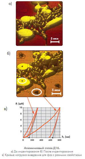
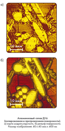
The study of the properties of multiphase materials implies precise positioning of the indentor in defined surface areas corresponding to the individual constituent components. Scanning nanohardometer "NanoScan" combines the functions of a scanning probe microscope and a hardness meter. The instrument's capabilities enable it to obtain a three-dimensional image of the surface topography of a multi-phase sample and then, with reference to the image obtained, precisely specify the measurement locations.
The accuracy of indentor positioning relative to the surface during measurements is in the order of 100 nm in the XY plane.
Example: sample of D16 aluminum alloy. Images of the topography of the same area of the sample surface before and after a series of measurements.
The accuracy of indentor positioning relative to the surface during measurements is in the order of 100 nm in the XY plane.
Example: sample of D16 aluminum alloy. Images of the topography of the same area of the sample surface before and after a series of measurements.
Measurement of the modulus of elasticity of materials by power spectroscopy
A method for measuring the absolute value of the modulus of elasticity of materials has been developed on the basis of NanoScan. The method of measurement consists in that a probe probe oscillating in the direction normal to the sample surface with an amplitude of less than
10 nm and a frequency of ~10 kHz is introduced into contact with the surface. As a result of the interaction of the indentor with the material, the probe oscillation frequency increases as it is pressed to the surface.In accordance with the mathematical description based on the Hertz model, the slope of the dependence of oscillation frequency on the penetration depth (approach curve) is proportional to the elasticity modulus of the material under study. Before measurements, calibration on reference materials with a known value of the modulus of elasticity is carried out. The elastic modulus value is determined by the ratio of the slope angles of the approach curves for the material under test and the reference materials.
The method is nondestructive and allows correct measurements of elastic modulus of materials up to 1000 GPa in a near-surface layer less than 100 nm thick. In particular, it is possible to measure the elastic modulus of thin films without introducing substrate influences. Comparative measurements carried out on different materials confirm the possibility of correct application of the described method in a wide range of values of the modulus of elasticity.
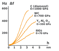
The slope of the resulting curve Δf characterizes the modulus of elasticity of the sample.
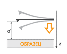
The "approach curve" measurement scheme.
To control the stiffness of beams and membranes, the scanning nanohardometer "NanoScan-4D" uses the mode of measuring load-displacement relations, similar to the method of measuring indentation. As a result of such a test, it is possible to determine stiffness (compliance) of the membrane or beam, maximum deflection of the membrane, and the number of load cycles before failure.
The NanoScan-4D uses a high-resolution digital optical microscope and a mode of preliminary scanning of the object surface before the test to accurately position the test point.
Fields of application: MEMS, NEMS
*Hardness measurement by measuring indentation method according to ISO14577
The NanoScan-4D uses a high-resolution digital optical microscope and a mode of preliminary scanning of the object surface before the test to accurately position the test point.
Fields of application: MEMS, NEMS
*Hardness measurement by measuring indentation method according to ISO14577
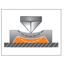
Scheme for measuring membrane properties.
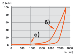
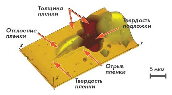
The sclerometry method (scratch application and analysis) has several advantages over indentation methods for measuring the hardness of films at the nanoscale. Direct observation of the residual scratch mark by the SPM method minimizes the effects of the predominant elastic deformation characteristic of indentation methods. Scratching with a variable load makes it possible to determine several film parameters in a single measurement procedure: the elastic interaction area, the threshold load at which plastic deformation begins (a visible trace appears on the surface), delamination and delamination of the film.
Mechanical properties of thin films
Thin films are actively used as protective and wear-resistant coatings for a wide range of objects. Correct measurement of mechanical properties of such films without influence of a substrate is a topical task in modern quality control systems. NanoScan-4D SZM allows to measure film hardness by different methods for a wide range of thicknesses. The most common method of measuring physical and mechanical properties of thin films today is the method of measuring indentation, implemented in NanoScan-4D. However, there are a number of factors that lead to methodological errors for this measurement method. The most critical of them are surface roughness, residual stresses and the so-called "substrate effect", which consists in the fact that for the film-substrate system the registered material response during measurement depends on both the film properties and the substrate properties.
Loading/unloading curve: stiffness and deflection of the membrane (a), resting of the membrane on the substrate (b).
Diamond-like film on a silicon substrate
Measuring the stiffness of beams and diaphragms

Hardness Measurement
from the image of the reconstructed print
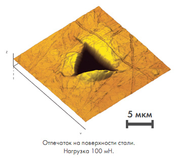
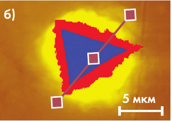
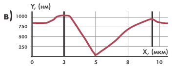
Scanning nano-hardness tester "NanoScan-4D" allows to carry out hardness testing by the method of reduced imprint (GOST 9450-76). In contrast to classical microhardness testers, measurement of the size of the print is made in the mode of semicontact scanning probe microscopy (SPM). Imprinting of a print and obtaining of its three-dimensional image are performed by the same probe probe in the framework of a single measuring procedure.A diamond indenter shaped as a trihedral Berkovich pyramid with an angle at the apex of 140° and a tip radius of ~50 nm is used as a tip. The recovered indentation hardness is calculated as the ratio of the maximum load applied to the indenter to the projection area of the recovered indentation measured from its image:
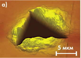
When plastic piles form around the perimeter of the recovered print, a three-dimensional image of the print allows you to determine their area and take them into account when calculating hardness values (Fig. 1). A special software module was implemented for automated measurement of the footprint area including heaps (Fig. 2). Applications: The proposed method can be used as a classical reconstructed indentation method in the area of small loads and depths, as well as to take into account the contribution of plastic heaps in the measuring indentation method (ISO 14577).
Mechanical nanolithography
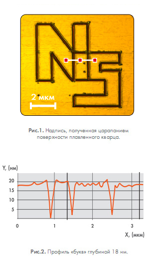
The devices of the NanoScan series offer a wide range of possibilities for precision mechanical micromachining and nanolithography. The use of diamond indenters makes it possible to cut almost any known material. By controlling the pressing force during cutting with resolution from 10 μN, it is possible to obtain scratches with width of 100 nm and depth of several nanometers steadily. The maximum scratch depth can reach several micrometers. By using precise piezo-ceramic nanopositioners and mechanical linear translators, the positioning accuracy of the diamond indenter reaches 10 nm in the 100 x 100 µm field and about 100 nm in the 100 x 100 mm field.
The result of surface micromachining can be monitored with the same diamond indenter by scanning in probe microscope mode or using a digital optical microscope.
The mechanical nanolithography mode can be used to create regular structures on the surface, remove oxide films, release coatings in specified areas, and correct the geometry of microelectronic components as well as micromechanical systems (MEMS).
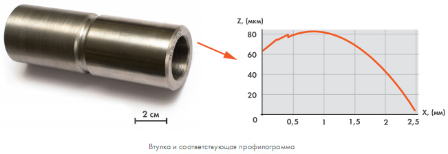
Surface profile measurement on a linear base up to 100 mm
In the profilometer mode, the scanning nanosurface tester "NanoScan-4D" allows to measure the surface profile on a linear base up to 100 mm. The height difference of the surface topography available for measurements is 10 mm. Horizontal resolution of the profilogram is 100 nm, vertical - 10 nm. The surface profilogram is measured in the semicontact mode of operation of the device probe. The force on the surface during measurements does not exceed 1 μN, which does not cause deformation of the surface.
Fields of application:
Fields of application:
- Operational control of the surface roughness of products.
- Control of the shape of complex surfaces.
- Searching and positioning of small objects.
- Determination of flatness and plane-parallelism of plates.
The modification of the nickel film surface was performed in a similar way. In this case, a sharper probe made of boron-doped diamond was used, pulse voltage 20 V, duration 1 ms. Figure 3a illustrates the nickel oxide nanostructures grown on the surface of the nickel film.
Electric probe lithography
Not only the geometric characteristics of the surface can be changed using the Electric Probe Lithography (EPL) method, but also its electrophysical properties. Applying a potential difference between the sample and the conductive probe causes electrochemical processes to occur under the tip of the probe, resulting in local oxidation of the substrate material and changes in conductivity, as well as causing changes in the surface shape, since the resulting oxides either have a larger volume or, conversely, are gaseous and vaporize. Using the software, it is possible to arrange the probe movement along a complex trajectory and form complex objects. EFL consisted of applying periodic pulses of high voltage between the probe and the sample in the mode of scanning and taking electrical signals. Due to the application of current between the probe and the film, localized heating of the surface under the tip of the probe and an electrochemical reaction of anodization of the material took place. Due to the presence of a liquid layer on the film surface, the reaction shifts towards oxidation due to the injection of electrons from the probe and the outflow of positive hydrogen ions to the probe. EFL was performed on iron and nickel films obtained by magnetron sputtering on the surface of a glass plate. For iron, the chemical equation of the reaction is as follows:

The experiment was carried out using a high-voltage pulse generator (pulse voltage - 60 V, duration 1 ms) Pulses were applied in random places of the surface. Then the sample was re-scanning and identification of modified areas. Figure 1 shows the surface topography of the iron film after EFL. Figure 2 illustrates the cross-sectional profile of the surface, the relief of the oxide formed as a consequence of EFL is clearly expressed, the height of the oxide film is from 25 to 70 nm.
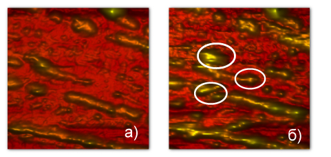
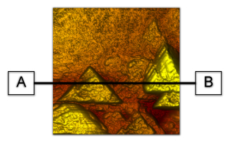
Figure 1: Surface topography. Fe2O3 nanostructures grown by applying high voltage pulses on the surface of the iron film on glass. Image size: 6.5 µm x 6.5 µm x 120 nm
Figure 3. a) Initial surface topography. b) Surface topography after modification, markers indicate nickel oxide islands formed by pulses. Image size: 6.5 µm x 6.5 µm x 120 nm
© 2023 Scanning nanohardness,
microhardness testers NanoScan
microhardness testers NanoScan

